Mega Plus PCB, Inc.

(714) 292-9919   (714) 550-0265

        sales@megapluspcb.com


Choosing Between Single-Sided, Double-Sided, and Multilayer Flex PCB Types: A Complete Comparison Guide


  April 15, 2025    |      Mega Plus PCB

Selecting the right flexible printed circuit board (flex PCB) is more than just choosing the number of conductive layers; it is a decision that directly influences electrical performance, mechanical flexibility, manufacturing complexity, reliability, and overall project cost. Whether you're designing a compact wearable device, an automotive control module, or a high-density medical system, choosing the wrong flex PCB type can result in unnecessary design constraints and increased manufacturing costs. Therefore, it is crucial for engineers to figure out whether a single-sided flex PCB, double-sided flex PCB, or multilayer flex PCB is the most suitable option during product development. While all three belong to the same family of flexible circuits, each is designed to solve different engineering challenges. This post provides a comprehensive single-sided vs double-sided vs multilayer flex PCB comparison, and key decision factors to help you choose the most appropriate flex PCB types for your next project.


rapid pcb prototyping

What is a Single-Sided Flex PCB?
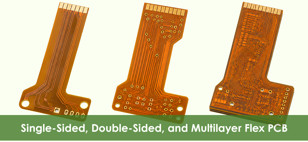
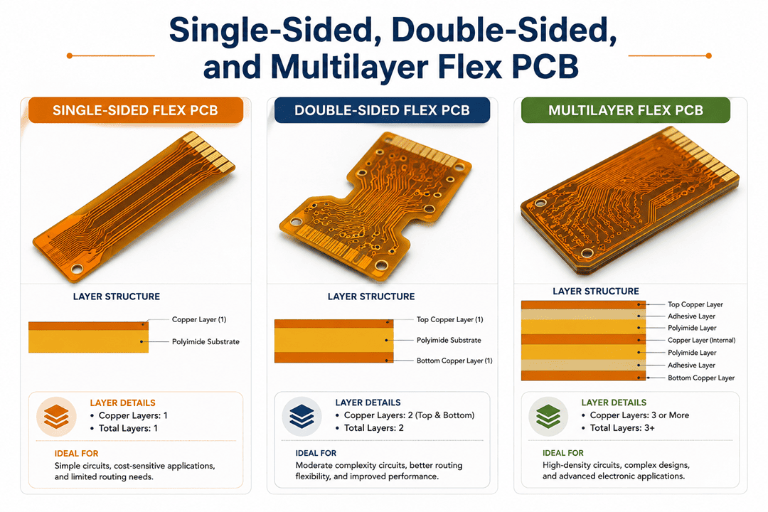
A single-sided flex PCB consists of one conductive copper layer bonded to a flexible dielectric substrate, typically polyimide, with a protective coverlay over the circuitry. Components and traces are placed on one side, making it the simplest and most cost-effective flex PCB design.


What is a Double-Sided Flex PCB?
A double-sided flex PCB has conductive copper layers on both sides of the flexible substrate, connected through plated through-holes (PTHs) or vias. This design increases routing capacity while maintaining flexibility for space-constrained applications. With access to both sides, it supports higher component density and more efficient circuit layouts without significantly increasing board size.

What is a Multilayer Flex PCB?
A multilayer flex PCB contains three or more conductive layers separated by flexible insulating materials and connected through plated vias. This structure supports complex circuit architectures, improved signal integrity, and higher electrical performance. Multilayer flex PCBs allow multiple circuit functions to be integrated into a single assembly, reducing the need for extra connectors and wiring.


Single-Sided vs Double-Sided vs Multilayer Flex PCB: Comprehensive Comparison

The table below compares the key technical, mechanical, and manufacturing differences between single-sided, double-sided, and multilayer flex PCBs.

Comparison Factor Single-Sided Flex PCB Double-Sided Flex PCB Multilayer Flex PCB
Circuit Complexity Best suited for simple and low-density circuit designs Supports moderately complex circuits with improved interconnections Designed for highly complex, high-density circuit layouts
Routing Capability Limited routing paths due to single-layer construction Improved routing through both sides of the substrate Extensive routing capacity across multiple internal and external layers
Component Placement Components are typically mounted on one side only Allows component placement on both sides for improved space utilization Supports high-density component placement across multiple layers and surfaces
Design Flexibility Offers the highest flexibility due to its thin and simple structure Maintains good flexibility with additional routing capability Provides moderate flexibility because of increased thickness and layer count
Dynamic Flex Performance Performs exceptionally well in repeated bending applications Suitable for moderate dynamic flex applications Better suited for limited or low-cycle flexing due to structural complexity
Bend Radius Supports the tightest bend radius for compact and flexible designs Requires a slightly larger bend radius due to dual copper layers Requires the largest bend radius because of thicker multilayer construction
Board Thickness Thinnest overall construction for lightweight designs Slightly thicker than single-sided designs Thickest construction due to multiple stacked layers
Weight Lightest weight, ideal for compact portable electronics Slightly heavier but still lightweight Heavier because of additional copper and dielectric layers
Signal Integrity Suitable for basic signal requirements and lower frequencies Improved signal performance with better routing options Offers advanced signal integrity for high-speed and complex electronic systems
EMI Control Limited EMI management options due to simpler construction Better EMI control through improved trace separation Enhanced EMI control through internal grounding and shielding layers
Power Distribution Supports basic power routing requirements Handles moderate power distribution more efficiently Supports advanced power management and complex power planes
Thermal Management Limited heat dissipation due to simple construction Better thermal handling than single-sided designs Improved heat distribution across multiple conductive layers
Mechanical Strength Good structural stability for lightweight applications Higher mechanical strength with dual-sided support Highest structural strength for demanding and rugged applications
Manufacturing Complexity Easiest and fastest to manufacture Requires additional processing steps for vias and alignment Most complex manufacturing process with precise layer registration
Production Lead Time Shortest lead times due to simpler fabrication Moderate lead times depending on design complexity Longer lead times because of multiple lamination and testing stages
Testing Complexity Simple testing due to limited circuitry More detailed testing for dual-layer interconnections Comprehensive testing required for multiple layers and vias
Repairability Easier to inspect and repair if issues occur Moderate repair complexity More difficult to repair due to internal circuit layers
Cost Most cost-effective option for simple designs Moderately priced for balanced performance and complexity Highest cost due to advanced materials, fabrication, and assembly requirements
Typical Applications Wearables, sensors, LED strips, and basic compact electronics Automotive modules, industrial controls, and consumer electronics Aerospace systems, medical devices, defense electronics, and high-density applications


Key Questions to Ask Before Finalizing Your Flex PCB Design

Before selecting the right flex PCB configuration, engineers should evaluate the following:

  • How complex is the circuit design?
  • Does the application require simple routing or high-density interconnections?
  • Will the PCB experience dynamic flexing, static bending, or remain fixed?
  • How much mechanical flexibility is required?
  • What are the space and size constraints of the final product?
  • Is higher component density required?
  • Are signal integrity, impedance control, or EMI management critical?
  • What are the operating temperature and environmental conditions?
  • How important are durability and long-term reliability?
  • What are the manufacturing cost and lead time limitations?
  • Does the application require lightweight construction?
  • Will future design scalability or additional circuit integration be needed?

Answering these questions early helps ensure the selected flex PCB type aligns with both performance requirements and manufacturing goals.


Turn Complex Flex PCB Designs into Reliable Production with Mega Plus PCBs

Choosing the right flex PCB configuration is only the first step. Ensuring it performs reliably in real-world applications requires the right manufacturing expertise. Whether you need single-sided, double-sided, or multilayer flex circuits, Mega Plus PCBs delivers the engineering support, precision manufacturing, and quality control needed to bring complex designs to life.

Request a Quote


FAQs

Are multilayer flex PCBs always better for complex electronics?

Not always. While multilayer flex PCBs offer higher routing capacity and advanced performance, they also increase manufacturing complexity and cost. The best choice depends on the application’s electrical and mechanical requirements.

Can double-sided flex PCBs reduce product size?

Yes. By utilizing both sides of the substrate for routing and component placement, double-sided Flex PCBs can improve space efficiency and support more compact product designs.

How does flex PCB layer count affect manufacturing cost?

As the layer count increases, fabrication becomes more complex due to added lamination, via formation, alignment, and testing requirements. This typically results in higher manufacturing costs and longer lead times.

What is the difference between dynamic flex and static flex applications?

Dynamic flex applications involve continuous or repeated bending during operation, while static flex applications are bent into position only once or infrequently. This distinction is critical when selecting the PCB structure and materials.

How do engineers choose between different flex PCB types for a new design?

Selecting between different flex PCB types depends on several factors, including circuit complexity, flexibility requirements, space constraints, operating environment, and long-term reliability expectations.