|
Printed Wiring Board vs Printed Circuit Board – Know the Real Difference
|
|
|
|
April 24, 2025 | Mega Plus PCB
In the electronics manufacturing industry, the terms printed wiring board (PWB) and printed circuit board (PCB) often create confusion among engineers, designers, and even decision-makers. While they appear interchangeably in various technical documents, they represent subtly different concepts that reflect the evolution of electronic board technology. Understanding PWB vs PCB is essential for professionals involved in design, prototyping, and small- and large-scale production of electronic devices. This post discussess a comprehensive analysis of PWB and PCB, highlighting their definitions, differences, and the reasons behind the global adoption of PCB terminology.
|
|
|
|
What is PWB?
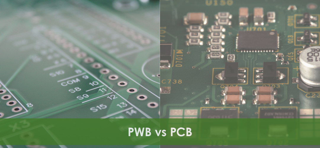
A printed wiring board represents the physical substrate that provides electrical connections between components through conductive pathways. The term emphasizes the wiring aspect, the copper traces and interconnections etched onto an insulating board material. Historically, PWB terminology focused on the board's primary function as an interconnection platform, essentially replacing traditional point-to-point wiring with printed conductive patterns.
What is PCB?
A printed circuit board includes the substrate and the complete circuit assembly with mounted components, such as resistors, capacitors, integrated circuits, and connectors. This definition reflects a fully functional system rather than only interconnection pathways. Modern PCB design also incorporates mechanical support, thermal management, electromagnetic shielding, and signal integrity requirements in addition to electrical connectivity.
|
|
|
|
Key Differences Between PWB and PCB
Here are the key differences between printed wiring board vs printed circuit board.
| Feature |
PWB (Printed Wiring Board) |
PCB (Printed Circuit Board) |
| Component Integration |
In a printed wiring board, components are mounted primarily for physical assembly with limited circuit-level integration. |
In a printed circuit board, components such as resistors, capacitors, and ICs are fully integrated to enable operational electronic performance. |
| Design Complexity |
A printed wiring board is typically designed with simpler layouts focused on basic wiring requirements. |
A printed circuit board supports complex multilayer architectures designed for high-performance electronic applications. |
| Manufacturing Approach |
A printed wiring board involves basic fabrication processes focused on creating conductive traces on a substrate. |
A printed circuit board involves advanced manufacturing processes including multilayer lamination, surface mounting, and precision etching. |
| Industry Usage |
A printed wiring board is mainly associated with early-stage or legacy electronic systems. |
A printed circuit board is the industry standard used in modern electronic devices across multiple sectors. |
| Engineering Focus |
A printed wiring board focuses primarily on physical wiring layout rather than system-level performance. |
A printed circuit board focuses on electrical performance, signal integrity, and system reliability. |
| Technical Documentation |
PWD is found in older military and aerospace specifications |
PCB is standard terminology used in IPC standards and contemporary technical literature |
| Regulatory Standards |
PWD is associated with historical military specifications (MIL-SPEC) |
PCB is aligned with current IPC, ISO, and international standards |
|
|
|
|
Why PCB Replaced PWB in Modern Electronics
The electronics industry's transition from PWB to PCB terminology reflects several fundamental developments in manufacturing capabilities and design complexity:
- Increased Circuit Complexity: Modern devices demand higher functionality in smaller spaces. Early PWBs were adequate for simple circuits, but as technology evolved, the need for multilayer boards with high-density interconnections became essential. PCBs accommodate these demands efficiently, providing reliable signal routing, reduced interference, and the ability to integrate complex components like microcontrollers and sensors.
- Evolution of Manufacturing Technology: Advancements in fabrication processes enabled the integration of passive components within board layers, embedded resistors and capacitors, and advanced materials for high-frequency applications. This evolution necessitated terminology that reflected the board's role as a complete circuit platform rather than a simple wiring substrate.
- Global Standardization Efforts: International standards organizations, particularly Institute for Printed Circuits (IPC), adopted PCB as the standard nomenclature in specifications and quality standards. This standardization facilitated clearer communication across multinational manufacturing operations and supply chains.
- Design Automation and CAD Systems: The development of sophisticated electronic design automation (EDA) software required consistent terminology. PCB became the universally recognized term in design software, simulation tools, and manufacturing systems, creating industry-wide linguistic uniformity.
- Functional Integration Requirements: Contemporary electronics demands boards that provide not only electrical connectivity but also thermal management, mechanical support, electromagnetic compatibility (EMC), and signal integrity. PCB terminology encompasses these multifunctional requirements more comprehensively than the limited scope of PWB.
- Documentation Consistency: Engineering teams, procurement departments, and quality assurance professionals benefit from standardized terminology that eliminates ambiguity in specifications, purchase orders, and technical communications. PCB has emerged as this universal standard.
- Educational and Professional Training: Academic institutions and professional certification programs standardized their curricula around PCB terminology, ensuring that new generations of engineers and technicians employ consistent language throughout their careers.
Are you looking for reliable and high-performance PCB solutions for complex electronic applications? Partnering with an experienced manufacturer ensures precision, rapid prototyping, and compliance with global standards.
Mega Plus PCB specializes in delivering high-quality, performance-driven PCB solutions tailored to complex engineering requirements. The company offers expertise in flex pcb, rigid-flex pcb, and FR4 technologies, supporting industries such as aerospace, medical, automotive, and telecommunications. Contact the experts today and discuss your requirement.
Request a Quote
|
|
|
|
FAQs
How does layer count impact PCB performance?
The number of layers in a PCB directly affects its routing capacity and signal performance. Higher-layer PCBs allow better space optimization, improved signal integrity, and support for more complex electronic designs.
What role does PCB surface finishing play in manufacturing?
Surface finishing protects exposed copper and ensures solderability during assembly. Common finishes like HASL, ENIG, and OSP enhance durability, corrosion resistance, and long-term electrical reliability.
How does PCB prototyping benefit product development?
PCB prototyping allows engineers to test and validate circuit functionality before mass production. It helps identify design flaws early, reduces development costs, and improves overall product reliability.
Why is impedance control important in PCB design?
Impedance control is critical for maintaining signal integrity in high-speed circuits. It helps minimize signal loss, reflections, and interference, ensuring reliable performance in advanced electronic applications.
|
|
|
|
|